
如何提高DC-DC转换器的效率
与底侧冷却封装相比,我们研究了具有顶侧冷却的表面安装(SMD)封装中的硅MOSFET的热性能。 本文分析了具有顶侧冷却的表面安装(SMD)封装中的硅MOSFET与底侧冷却封装相比在热性能方面的效率,降低了热阻和工作温度。它将展示降低结温度如...
与底侧冷却封装相比,我们研究了具有顶侧冷却的表面安装(SMD)封装中的硅MOSFET的热性能。
本文分析了具有顶侧冷却的表面安装(SMD)封装中的硅MOSFET与底侧冷却封装相比在热性能方面的效率,降低了热阻和工作温度。它将展示降低结温度如何有助于提高功率效率,这是由于温度变化(如RDS)导致主硅MOSFET参数的更平滑变化(开)以及Vth电平,并且减少了总的导通和开关损耗。
介绍
电力转换产品市场正在迅速现代化,以应对电力生产和管理方式的变化。此外,由于电力正在增加,为各种具有不同特性和要求的巨大且快速扩展的负载供电。这种现代化正在推动功率转换器在各个阶段的重新设计,以满足提高功率密度和功率效率、更好的热管理以及减轻重量和尺寸的需求。在某些情况下,转换器需要实现双向性。
DC/DC转换器概述
功率转换器的DC/DC级是电源的关键部分。该级将输入恒定电压转换为受控的DC输出电压,该输出电压可以高于或低于输入,这取决于转换器是降压转换器还是升压转换器。DC/DC转换器可以是具有固定输入和输出级的单向转换器,也可以是具有可互换输入和输出的双向转换器。
图1和图2显示了半桥(HB)LLC谐振和全桥(FB)相移转换器最常见的单向拓扑结构。
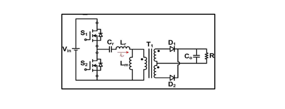
<img data-lazy-fallback="1" decoding="async" src="https://uploads.9icnet.com/images/aritcle/20230421/HB-LLC-unidirectional-power-electronics-news.png" alt="HB LLC, unidirectional.">
图1:HB有限责任公司,单向
<img data-lazy-fallback="1" decoding="async" src="https://uploads.9icnet.com/images/aritcle/20230421/full-bridge-phase-shift-unidirectional-converter-power-electronics-news.png" alt="full-bridge phase shift, unidirectional converter.">
图2:全桥相移,单向转换器。
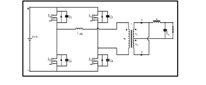
图3和图4显示了双向拓扑结构。
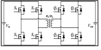
<img data-lazy-fallback="1" decoding="async" src="https://uploads.9icnet.com/images/aritcle/20230421/Dual-active-bridge-bidirectional-converter-power-electronics-news.png" alt="Dual active bridge, bidirectional converter.">
图3:双有源桥,双向转换器。
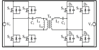
<img data-lazy-fallback="1" decoding="async" src="https://uploads.9icnet.com/images/aritcle/20230421/CLLLC-bidirectional-converter-power-electronics-news.png" alt="CLLLC, bidirectional converter.">
图4:CLLLC,双向转换器。
这些不同的拓扑结构有一个共同的特点:它们都在导通时使用零电压开关(ZVS)来降低开关损耗。
底侧和顶侧冷却SMD封装
MOSFET和IGBT等功率器件,包括普通硅以及宽带隙碳化硅(SiC)和氮化镓(GaN)器件,都封装在设计用于防止潮湿和外部污染以及确保电隔离的封装中。
与通孔相比,现在的市场趋势是表面安装(SMD)封装样式,因为它们允许:
表面贴装封装可分为:
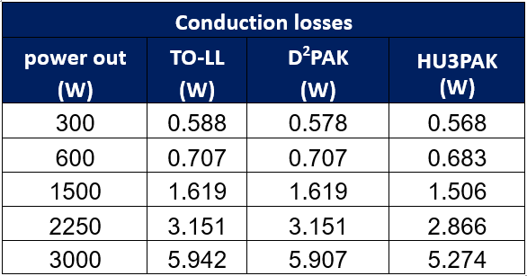
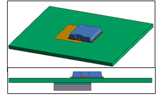
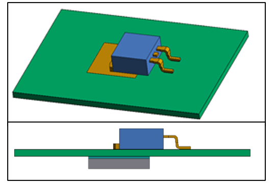
该评估将HU3PAK顶侧冷却组件的热性能与D的热性能进行了比较2.PAK和TO-LL底侧冷却包在相同的工作和热系统条件下。
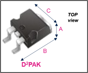
<img data-lazy-fallback="1" decoding="async" src="https://uploads.9icnet.com/images/aritcle/20230421/D2PAK-Power-electronics-news.png" alt="D2PAK.">
图5:D2.巴基斯坦
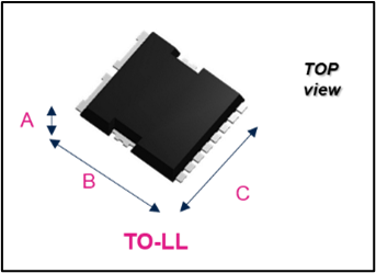
<img data-lazy-fallback="1" decoding="async" src="https://uploads.9icnet.com/images/aritcle/20230421/TO-LL-Power-electronics-news.png" alt="TO-LL">
图6:TO-LL
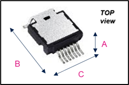
<img data-lazy-fallback="1" decoding="async" src="https://uploads.9icnet.com/images/aritcle/20230421/HU3PAK-power-electronics-news.png" alt="HU3PAK.">
图7:HU3PAK
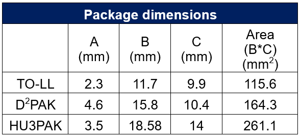
<img data-lazy-fallback="1" decoding="async" src="https://uploads.9icnet.com/images/aritcle/20230421/package-dimensions-d2pak-toll-hu3pak-power-electronics-news.png" alt="Package dimensions and occupation of area on PCB.">
表1:PCB上的封装尺寸和占地面积。
功率损耗分析
本节介绍了方程[1-4]和初步功率损耗。这些功率损耗为SMD封装的热建模和分析提供了输入数据。测试车辆为3kW全桥LLC变流器。从方程1、2、3和4[1]开始,在五个负载点评估初级MOSFET损耗:最大功率(3kW)的10%、20%、50%、75%和100%。表2总结了损失情况。
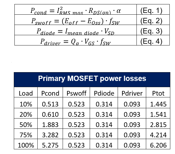
<img data-lazy-fallback="1" decoding="async" src="https://uploads.9icnet.com/images/aritcle/20230421/primary-mosfets-power-losses-power-electronics-news.png" alt="MOSFET power losses at different load points">
表2:不同负载点的MOSFET功率损耗
开关损耗、驱动器损耗和二极管损耗是相同的,因为功率损耗模型在谐振频率下计算它们。
功率损耗的第一次分析有助于找出硅在结温度(Tj)方面的工作点。三种不同包装内的设备,D2.PAK、TO-LL和HU3PAK是相同的。设备具有RDS(开)在25°C时等于80 mΩ。
在下一段中,热分析发现,由于结与环境热阻(RthJA)包裹的数量。
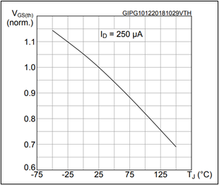
因此,不同的结温会影响RDS(开)以及栅极阈值电压(VGSth)。
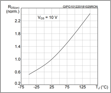
<img data-lazy-fallback="1" decoding="async" src="https://uploads.9icnet.com/images/aritcle/20230421/rdson-behaviour-vs-Tj-power-electronics-news.png" alt="RDS(on) behavior vs Tj. The curve represents the thermal multiplicative factor.">
图8:RDS(开)行为与Tj。该曲线表示热倍增因子。
<img data-lazy-fallback="1" decoding="async" src="https://uploads.9icnet.com/images/aritcle/20230421/VGSth-behavior-vs-Tj-power-electronics-news.png" alt="VGSth behavior vs Tj.">
图9:VGSth行为与Tj。
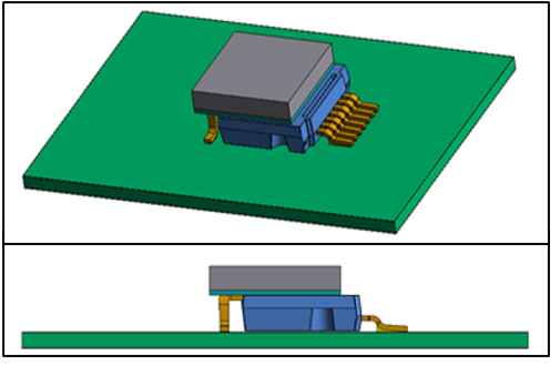
Tj对RDS的影响要大得多(开)与VGSth相比。因此,仅根据Tj值和不同的RDS来计算传导损耗(开)价值观表3报告了RDS的乘法系数(开)三种不同的包装。
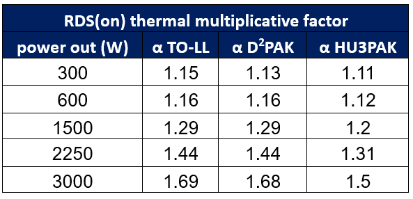
<img data-lazy-fallback="1" decoding="async" src="https://uploads.9icnet.com/images/aritcle/20230421/RDSon-thermal-multiplicative-factor-power-electronics-news.png" alt="Thermal coefficient to consider the increase of RDS(on) vs Tj.">
表3:考虑RDS增加的热系数(开)与Tj相比。
<img data-lazy-fallback="1" decoding="async" src="https://uploads.9icnet.com/images/aritcle/20230421/Conduction-Losses-power-electronics-news.png" alt="Conduction losses for all three packages at different RDS(on) values.">
表4:不同RDS下所有三个包的传导损耗(开)价值观
HU3PAK的结果证实,当在与其他封装相同的功率水平下运行时,该顶侧冷却封装保持较低的结温度。因此,它消耗的功率较少,从而提高了整体功率效率(因为RDS(开)在较高的结温下升高(参考图8)。因此,确保较低Tj的更具热效率的封装有助于最小化功率损耗)。
热模拟和分析
本节重点介绍为验证顶侧冷却解决方案而进行的热模拟。使用数值有限元方法进行了模拟。这种方法可以评估通过热界面材料(TIM)连接到印刷电路板(PCB)的功率MOSFET的热行为。模拟中使用的功率损耗来自实际操作条件(轻载和满载时的DC/DC转换器),如前一节所示。
已经进行了模拟基准测试,考虑了三种一揽子解决方案:D2.PAK和TO-LL作为底侧冷却,HU3PAK作为顶侧冷却。本摘要所示的第一次评估是在稳定状态下进行的。模拟使用相同的散热器,放置在PCB的D热过孔的底部2.PAK和TO-LL,并在HU3PAK上的实验中直接在顶部暴露的铜框架上。
此外,同样的2层PCB(2盎司铜),具有热过孔、TIM和边界条件(Tamb=25°C,传热系数(Htc)=750 W/m2.散热器表面上的K)应用于所有物理模型。
<img data-lazy-fallback="1" decoding="async" src="https://uploads.9icnet.com/images/aritcle/20230421/Isometric-and-lateral-view-of-TO-LL-simulated-geometry-power-electronics-news.png" alt="Isometric and lateral view of TO-LL simulated geometry, PCB and heatsink on bottom side.">
图8:TO-LL模拟几何结构、PCB和底部散热器的等距和横向视图。
<img data-lazy-fallback="1" decoding="async" src="https://uploads.9icnet.com/images/aritcle/20230421/Isometric-and-lateral-view-of-D2PAK-simulated-geometry-PCB-and-heatsink-on-bottom-side-power-electronics-news.png" alt="Isometric and lateral view of D2PAK simulated geometry, PCB, and heatsink on bottom side.">
图9:D的等距和横向视图2.PAK模拟了底部的几何形状、PCB和散热片。
<img data-lazy-fallback="1" decoding="async" src="https://uploads.9icnet.com/images/aritcle/20230421/Isometric-and-lateral-view-of-HU3PAK-simulated-geometry-power-electronics-news.png" alt="Isometric and lateral view of HU3PAK simulated geometry, PCB, and heatsink on top side.">
图10:顶部HU3PAK模拟几何结构、PCB和散热器的等距和横向视图。
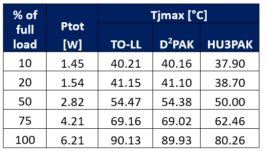
表5给出了第一次模拟的结果,以预测三个设备中每一个在10%、20%、50%、75%和100%满负荷时的Tjmax。结果如表5所示,证实了TO-LL和D的类似行为2.PAK,HU3PAK的温度更低。满载时温差更明显。
<img data-lazy-fallback="1" decoding="async" src="https://uploads.9icnet.com/images/aritcle/20230421/Tj-max-for-each-package-at-various-fractions-of-full-load-power-electronics-news.png" alt="Tj max for each package at various fractions of full load (same power losses for each package).">
表5:在满载的不同分数下,每个封装的Tj max(每个封装的功率损耗相同)。
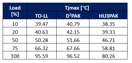
下一个实验对每个器件进行热模拟,考虑来自表4的更新的传导损耗。
图12显示了TO-LL、D全负荷时的模拟热图2.PAK和HU3PAK。
<img data-lazy-fallback="1" decoding="async" src="https://uploads.9icnet.com/images/aritcle/20230421/Packages-Tj-max-reach-for-each-load-percentage-power-electronics-news.png" alt="Packages Tj max reached for each load percentage (different power losses for each package).">
表6:每个负载百分比达到的封装Tj最大值(每个封装的不同功率损耗)。
<img data-lazy-fallback="1" decoding="async" src="https://uploads.9icnet.com/images/aritcle/20230421/temperature-comparison-load-percentage-power-electronics-news.png" alt="Temperature comparison for each load percentage">
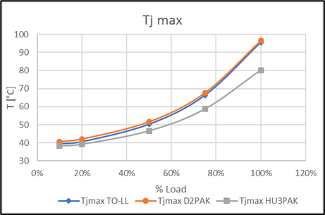
图11:每个负载百分比的温度比较
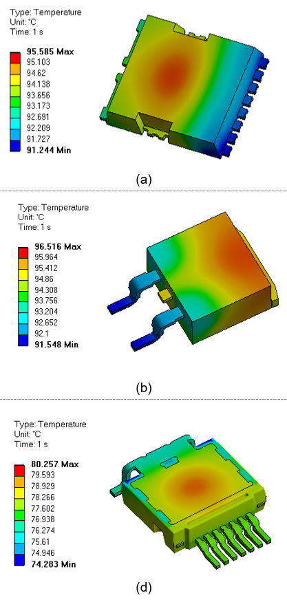
<img data-lazy-fallback="1" decoding="async" src="https://uploads.9icnet.com/images/aritcle/20230421/TO-LL-a-D2PAK-b-and-HU3PAK-c-thermal-map-at-steady-state-power-electronics-news.png" alt="TO-LL (a), D2PAK (b) and HU3PAK (c) thermal map at steady state.">
图12:TO-LL(a),D2.PAK(b)和HU3PAK(c)稳态热图。
结果表明,D2.PAK和TO-LL具有等效的热行为,而HU3PAK在相同的负载点达到较低的温度。
正如预期的那样,HU3PAK更好的热性能主要是由于顶部侧冷却。优越的热性能在满负荷时最为明显。
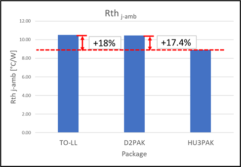
最后,Rthj-amb公司这证实了HU3PAK的性能优于其他两个包。
<img data-lazy-fallback="1" decoding="async" src="https://uploads.9icnet.com/images/aritcle/20230421/D2PAK-TO-LL-and-HU3PAK-RthJA-power-electronics-news.png" alt="D2PAK, TO-LL and HU3PAK RthJA.">
图13:D2.PAK、TO-LL和HU3PAK RthJA。
模型验证
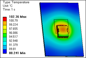
最后一步通过比较模拟和实验结果来验证模型[2],如图15所示。
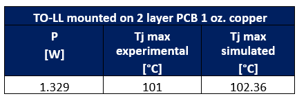
显示的设备是TO-LL。它安装在与上一段中进行的模拟中使用的PCB相同的PCB上,从而获得表7[2]中所示的结果。
关于边界条件,考虑了PCB下侧的绝热行为,传热系数(Htc)为11W/m2.K在封装和PCB的顶侧表面上。
<img data-lazy-fallback="1" decoding="async" src="https://uploads.9icnet.com/images/aritcle/20230421/Measured-and-simulated-values-of-Tj-max-for-TO-LL-package-power-electronics-news.png" alt="Measured and simulated values of Tj max for TO-LL package.">
表7:TO-LL封装的Tj最大值的测量值和模拟值。
该模型得到了验证,误差幅度小于1.5%,这表明模拟和实验测量之间有很好的一致性。
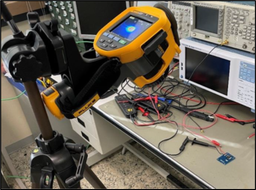
<img data-lazy-fallback="1" decoding="async" src="https://uploads.9icnet.com/images/aritcle/20230421/experiment-setup-for-measurement-power-electronics-news.png" alt="Experiment setup for measurement.">
图14:测量实验设置
<img data-lazy-fallback="1" decoding="async" src="https://uploads.9icnet.com/images/aritcle/20230421/Thermal-simulation-of-TO-LL-performed-for-model-validation-power-electronics-news.png" alt="Thermal simulation of TO-LL, performed for model validation.">
图15:TO-LL的热模拟,用于模型验证。
结论
HU3PAK封装具有顶侧冷却功能,与D等其他SMD封装相比显示出许多优势2.PAK和TO-LL。当与相同的散热器尺寸和PCB热特性(铜重量)一起使用时,由于其增加的散热能力,它允许更大的功率密度。
如图所示,HU3PAK降低了Rthj-amb公司相对于D中使用的更常见的底侧冷却方法,最多可减少18%2.PAK和TO-LL。
还要记住,模拟是在考虑的所有三个机组的相同冷却系统下进行的。然而,通过优化冷却系统,可以进一步提高HU3PAK的热性能。
工具书类
[1] D.Nardo,A.Scuto和S.Buonomo,“谐振LLC转换器中初级侧MOSFET损耗的评估”2021 PCIM欧洲数字日;国际电力电子、智能运动、可再生能源和能源管理展览会2021,第1-8页。
[2] G.毛罗米卡莱等.,“高压SMD封装冷却解决方案的建模和热分析”2021 PCIM欧洲数字日;国际电力电子、智能运动、可再生能源和能源管理展览会2021,第1-8页。
-Marco Papaserio、Domenico Nardo、Daniela Cavallaro、Cristiano Gianluca Stella和Stefano Orlando都在ST微电子公司工作。
>>这篇文章最初发表在我们的姐妹网站上,电力电子新闻.