- Density : 4G bits
- Organization : 32M words x 16 bits x 8 banks
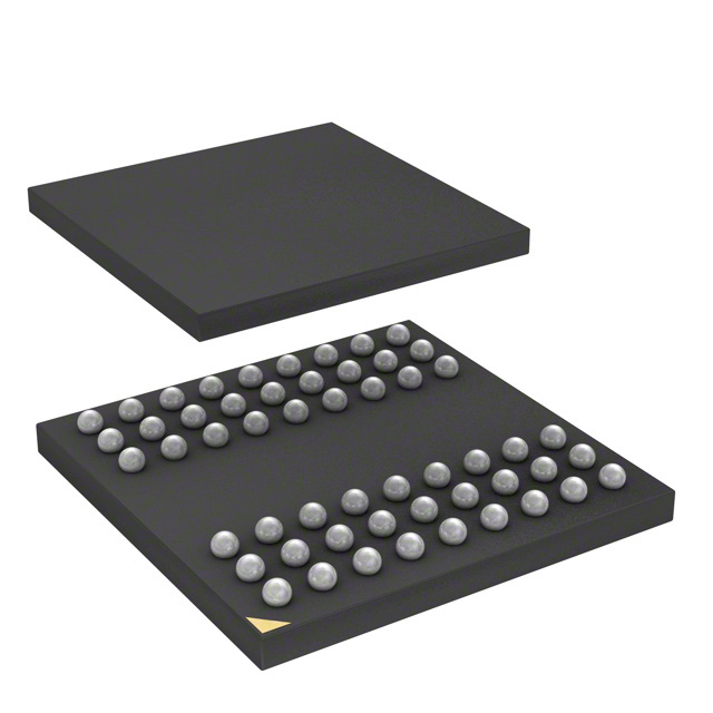
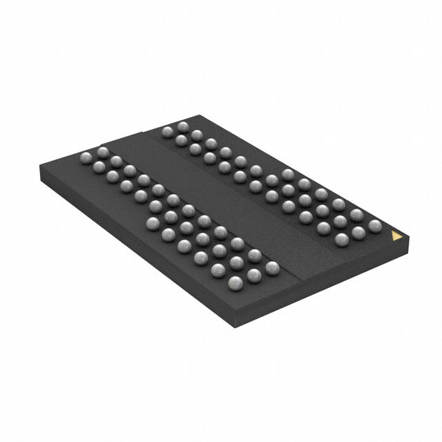
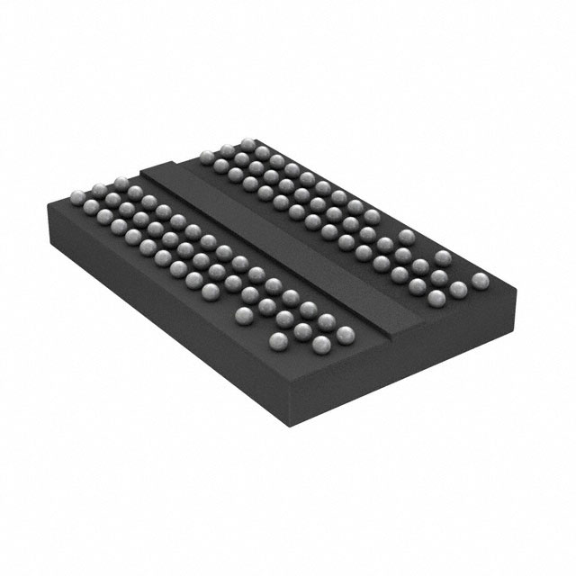
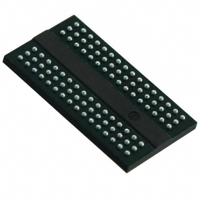
- Package :
- 96-ball FBGA
- Lead-free (RoHS compliant) and Halogen-free
- Power supply : VDD, VDDQ = 1.35V (1.283V to 1.45V)
- Backward compatible to VDD, VDDQ = 1.5V ± 0.075V
- Data rate :
- 1600Mbps
- 2KB page size
- Row address: A0 to A14
- Column address: A0 to A9
- Eight internal banks for concurrent operation
- Burst lengths (BL) : 8 and 4 with Burst Chop (BC)
- Burst type (BT) :
- Sequential (8, 4 with BC)
- Interleave (8, 4 with BC)
- CAS Latency (CL) : 5, 6, 7, 8, 9, 10, 11
- CAS Write Latency (CWL) : 5, 6, 7, 8
- Precharge : auto precharge option for each burst access
- Driver strength : RZQ/7, RZQ/6 (RZQ = 240 Ω)
- Refresh : auto-refresh, self-refresh
- Refresh cycles : - Average refresh period
7.8 μs at 0°C ≤ Tc ≤ +85°C
3.9 μs at +85°C < Tc ≤ +95°C
- Operating case temperature range
Commercial Tc = 0°C to +95°C
Features
- Double-data-rate architecture; two data transfers per clock cycle
- The high-speed data transfer is realized by the 8 bits prefetch pipelined architecture
- Bi-directional differential data strobe (DQS and DQS) is transmitted/received with data for capturing data at the receiver
- DQS is edge-aligned with data for READs; center-aligned with data for WRITEs
- Differential clock inputs (CK and CK)
- DLL aligns DQ and DQS transitions with CK transitions
- Commands entered on each positive CK edge; data and data mask referenced to both edges of DQS
- Data mask (DM) for write data
- Posted CAS by programmable additive latency for better command and data bus efficiency
- On-Die Termination (ODT) for better signal quality
- Synchronous ODT
- Dynamic ODT
- Asynchronous ODT
- Multi Purpose Register (MPR) for pre-defined pattern read out
- ZQ calibration for DQ drive and ODT
- Programmable Partial Array Self-Refresh (PASR)
- RESET pin for Power-up sequence and reset function
- SRT range : Normal/extended
- Programmable Output driver impedance control
(Picture:Pinout / Diagram)