All trademarks are the property of their respective owners.
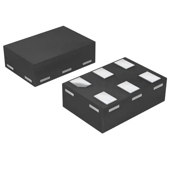
DescriptionThe LSF family consists of bidirectional voltage level translators that operate from 0.8V to 4.5 V (Vref_A) and 1.8 V to 5.5 V (Vref_B). This range allows for bidirectional voltagetranslations between 0.8 V and 5.0 V without the need for a direction terminal in open-drain orpush-pull applications. The LSF family supports level translation applications with transmissionspeeds greater than 100 MHz for open-drain systems that utilize a 15-pF capacitance and 165-Ωpull-up resistor.
When the An or Bn port is LOW, the switch is in the ON-state and a low resistanceconnection exists between the An and Bn ports. The low Ron of the switchallows connections to be made with minimal propagation delay and signal distortion. The voltage onthe A or B side will be limited to Vref_A and can be pulled up to any level between Vref_A and 5 V.This functionality allows a seamless translation between higher and lower voltages selected by theuser without the need for directional control.
The supply voltage (Vpu#) for each channel may be individuallyset up with a pull up resistor. For example, CH1 may be used in up-translation mode (1.2 V ? 3.3 V)and CH2 in down-translation mode (2.5 V ? 1.8 V).
When EN is HIGH, the translator switch is on, and the An I/O is connected to the Bn I/O,respectively, allowing bidirectional data flow between ports. When EN is LOW, the translator switchis off, and a high-impedance state exists between ports. The EN input circuit is designed to besupplied by Vref_A. EN must be LOW to ensure the high-impedance state during power-up orpower-down.
Feature
- Provides bidirectional voltage translation with no direction terminal
- Supports up to 100-MHz up translation and greater than 100-MHz down translationat ≤ 30-pF capacitor load and up to 40-MHz up/down translation at 50-pF capacitorload
- Supports Ioff, partial power-down mode (refer toFeature Description)
- Allows bidirectional voltage level translation between
- 0.8 V ? 1.8, 2.5, 3.3, 5 V
- 1.2 V ? 1.8, 2.5, 3.3, 5 V
- 1.8 V ? 2.5, 3.3, 5V
- 2.5 V ? 3.3, 5 V
- 3.3 V ? 5V
- Low standby current
- 5 V Tolerance I/O port to supportTTL
- Low Ron provides less signaldistortion
- High-impedance I/O terminals for EN = Low
- Flow-through pinout for easy PCB trace routing
- Latch-upperformance exceeds 100 mA per JESD17
- –40°C to 125°C operating temperature range
- ESD performancetested per JESD 22
- 2000-V human-body model (A114-B, Class II)
- 200-V machine model (A115-A)
- 1000-V charged-device model(C101)
All trademarks are the property of their respective owners.
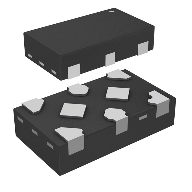
DescriptionThe LSF family consists of bidirectional voltage level translators that operate from 0.8V to 4.5 V (Vref_A) and 1.8 V to 5.5 V (Vref_B). This range allows for bidirectional voltagetranslations between 0.8 V and 5.0 V without the need for a direction terminal in open-drain orpush-pull applications. The LSF family supports level translation applications with transmissionspeeds greater than 100 MHz for open-drain systems that utilize a 15-pF capacitance and 165-Ωpull-up resistor.
When the An or Bn port is LOW, the switch is in the ON-state and a low resistanceconnection exists between the An and Bn ports. The low Ron of the switchallows connections to be made with minimal propagation delay and signal distortion. The voltage onthe A or B side will be limited to Vref_A and can be pulled up to any level between Vref_A and 5 V.This functionality allows a seamless translation between higher and lower voltages selected by theuser without the need for directional control.
The supply voltage (Vpu#) for each channel may be individuallyset up with a pull up resistor. For example, CH1 may be used in up-translation mode (1.2 V ? 3.3 V)and CH2 in down-translation mode (2.5 V ? 1.8 V).
When EN is HIGH, the translator switch is on, and the An I/O is connected to the Bn I/O,respectively, allowing bidirectional data flow between ports. When EN is LOW, the translator switchis off, and a high-impedance state exists between ports. The EN input circuit is designed to besupplied by Vref_A. EN must be LOW to ensure the high-impedance state during power-up orpower-down.