
Xilinx introduces the QPro™ XQ18V04VQ44N Military Grade 4Mbit in-system programmable configuration Flash PROM. The XQ18V04VQ44N is a 3.3V rewritable PROM that provides a reliable non-volatile method for storing large Xilinx FPGA configuration bitstreams used in systems that require operation over the full military temperature range.
When the FPGA is in Master Serial mode, it generates a configuration clock that drives the PROM. A short access time after the rising CCLK, data is available on the PROM DATA (D0) pin that is connected to the FPGA DIN pin. The FPGA generates the appropriate number of clock pulses to complete the configuration.
When the FPGA is in Slave Serial mode, the PROM and the FPGA are clocked by an external clock. When the FPGA is in SelectMAP mode (Slave), an external oscillator will generate the configuration clock that drives the PROM and the FPGA. After the rising CCLK edge, data is available on the PROMs DATA (D0-D7) pins. The data will be clocked into the FPGA on the following rising edge of the CCLK.
Multiple devices can be cascaded by using the CEO output to drive the CE input of the following device. The clock inputs and the DATA outputs of all PROMs in this chain are interconnected. The XQ18V04VQ44N is compatible and can be cascaded with other configuration PROMs such as the XQR1701L and XQR17V16 one-time programmable configuration PROMs.
Features
• Operating Temperature Range: –55°C to +125° C
• Low-power advanced CMOS FLASH process memory cells immune to static single event upset
• In-system programmable 3.3V PROMs for configuration of Xilinx FPGAs
- Endurance of 20,000 program/erase cycles
• IEEE Std 1149.1 boundary-scan (JTAG) support
• Cascadable for storing longer or multiple bitstreams
• Dual configuration modes
- Serial Slow/Fast configuration (up to 20 MHz)
- Parallel (up to 160 Mbps at 20 MHz)
• 5V tolerant I/O pins accept 5V, 3.3V, and 2.5V signals
• 3.3V or 2.5V output capability
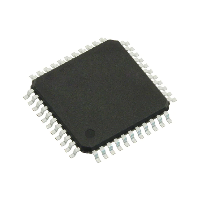
• Available in plastic VQ44 packaging only
• Design support using the Xilinx Alliance Series™ and Xilinx Foundation Series™ software packages
• JTAG command initiation of standard FPGA configuration
Feature
• Low-power advanced CMOS FLASH process memory cells immune to static single event upset
• In-system programmable 3.3V PROMs for configuration of Xilinx FPGAs
- Endurance of 20,000 program/erase cycles
• IEEE Std 1149.1 boundary-scan (JTAG) support
• Cascadable for storing longer or multiple bitstreams
• Dual configuration modes
- Serial Slow/Fast configuration (up to 20 MHz)
- Parallel (up to 160 Mbps at 20 MHz)
• 5V tolerant I/O pins accept 5V, 3.3V, and 2.5V signals
• 3.3V or 2.5V output capability
• Available in plastic VQ44 packaging only
• Design support using the Xilinx Alliance Series™ and Xilinx Foundation Series™ software packages
• JTAG command initiation of standard FPGA configuration


