The NLSF3T126MNR2 is a high speed CMOS quad bus buffer fabricated with silicon gate CMOS technology. It achieves high speed operation similar to equivalent Bipolar Schottky TTL while maintaining CMOS low power dissipation.The NLSF3T126MNR2 requires the 3-state control input (OE)to be set Low to place the output into the high impedance state.The T126 inputs are compatible with TTL levels. This device can be used as a level converter for interfacing 3.3 V to 5.0 V, because it has full 5.0 V CMOS level output swings. The NLSF3T126MNR2 input structures provide protection when voltages between 0 V and 5.5 V are applied, regardless of the supply voltage. The output structures also provide protection when VCC = 0 V. These input and output structures help prevent device destruction caused by supply voltage - input/output voltage mismatch, battery backup, hot insertion, etc. The internal circuit is composed of three stages, inculding a buffer output which provides high noise immunity and stable output. The inputs tolerate voltages up to 7.0 V, allowing the interface of 5.0 V systems to 3.0 V systems.
Feature
- High Speed: tpD = 3.8 ns (Typ) at VCC = 5.0 V
- Low Power Dissipation: ICC = 4.0 µA (Max) at TA = 25°C
- TTl-Compatible Inputs: VIL = 0.8 V; VIH = 2.0 V
- Power Down Protection Provided on Inputs
- Balanced Propagation Delays
- Designed for 2.0 V to 5.5 V Operating Range
- Low Noise: VOLP = 0.8 V (Max)
- Pin and Function Compatible with Other Staqndard Logic Families
- latch up Performance Exceeds 300 mA
- ESD Performance: HBM > 2000 V; Machine Model > 200 V
- Chip Complexity: 72 FETs or 18 Equivalent Gates
- Pb-Free Package is Available
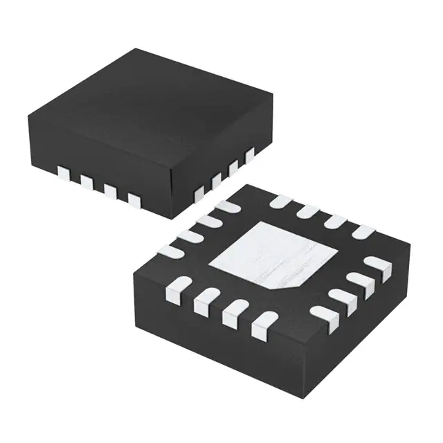
(Picture: Pinout)