The UJA1079A core System Basis Chip (SBC) replaces the basic discrete components commonly found in Electronic Control Units (ECU) with a Local Interconnect Network (LIN) interface.
The UJA1079A supports the networking applications used to control power and sensor peripherals by using the LIN interface as a local sub-bus.
The core SBC contains the following integrated devices:
- LIN transceiver compliant with LIN 2.1, LIN 2.0 and SAE J2602, and compatible with LIN 1.3
- Advanced independent watchdog (UJA1079A/xx/WD versions)
- 250 mA voltage regulator for supplying a microcontroller; extendable with external PNP transistor for increased current capability and dissipation distribution
- Serial Peripheral Interface (SPI) (full duplex)
- 2 local wake-up input ports
- Limp home output port
In addition to the advantages gained from integrating these common ECU functions in a single package, the core SBC offers an intelligent combination of system-specific functions such as:
- Advanced low-power concept
- Safe and controlled system start-up behavior
- Detailed status reporting on system and sub-system levels
The UJA1079A is designed to be used in combination with a microcontroller. The SBC ensures that the microcontroller always starts up in a controlled manner.
Feature
- Contains LIN ECU functions:
- LIN transceiver
- Scalable 3.3 V or 5 V voltage regulator delivering up to 250 mA for a microcontroller and peripheral circuitry; an external PNP transistor can be connected for better heat distribution over the PCB
- Watchdog with Window and Timeout modes and on-chip oscillator
- Serial Peripheral Interface (SPI) for communicating with the microcontroller
- ECU power management system
- Designed for automotive applications:
- Enhanced ElectroMagnetic Compatibility (EMC) performance
- ±8 kV ElectroStatic Discharge (ESD) protection Human Body Model (HBM) on the LIN bus pin and the wake-up pins
- ±6 kV ElectroStatic Discharge protection IEC 61000-4-2 on the LIN bus pin and the wake-up pins
- ±58 V short-circuit proof LIN bus pin
- Battery and LIN bus pins are protected against transients in accordance with ISO 7637-3
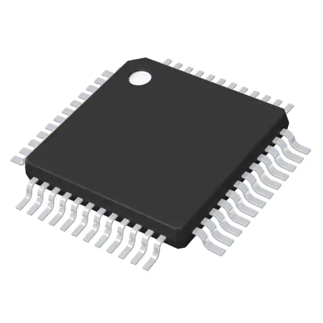
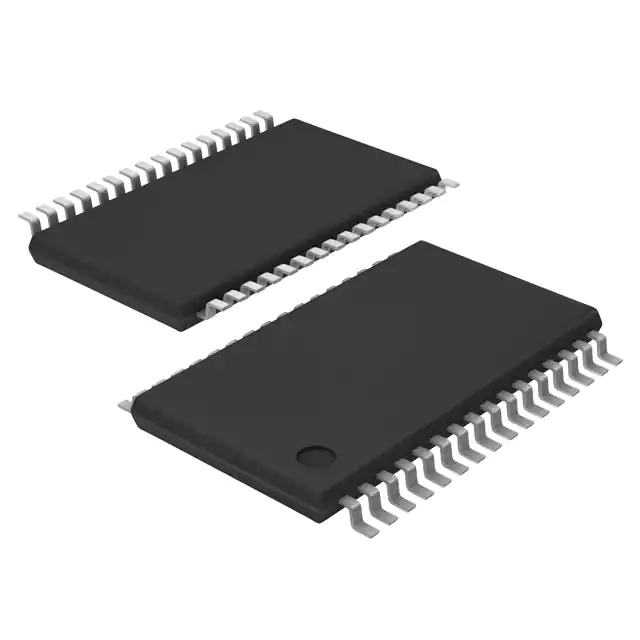
- Small 6.1 mm × 11 mm HTSSOP32 package with low thermal resistance
- Pb-free; Restriction of Hazardous Substances Directive (RoHS) and dark green compliant
- LIN 2.1 compliant LIN transceiver
- Compliant with SAE J2602
- Downward compatible with LIN 2.0 and LIN 1.3
- Low slope mode for optimized EMC performance
- Integrated LIN termination diode at pin DLIN
- Wake-up via LIN or local wake-up pins with wake-up source detection
- 2 wake-up pins:
- WAKE1 and WAKE2 inputs can be switched off to reduce current flow
- Output signal (WBIAS) to bias the wake-up pins, selectable sampling time of 16 ms or 64 ms
- Standby mode with very low standby current and full wake-up capability; V1 active to maintain supply to the microcontroller
- Sleep mode with very low sleep current and full wake-up capability
- Safe and predictable behavior under all conditions
- Programmable watchdog with independent clock source
- Window, Timeout (with optional cyclic wake-up) and Off modes supported (with automatic re-enable in the event of an interrupt)
- 16-bit Serial Peripheral Interface (SPI) for configuration, control and diagnosis
- Global enable output for controlling safety-critical hardware
- Limp home output (LIMP) for activating application-specific ‘limp home’ hardware in the event of a serious system malfunction
- Overtemperature shutdown
- Interrupt output pin; interrupts can be individually configured to signal V1 undervoltage, LIN/local wake-up and cyclic and power-on interrupt events
- Bidirectional reset pin with variable power-on reset length to support a variety of microcontrollers
- Software-initiated system reset
- Scalable voltage regulator for the microcontroller, its peripherals and additional external transceivers
- ±2 % accuracy
- 3.3 V and 5 V versions available
- Delivers up to 250 mA and can be combined with an external PNP transistor for better heat distribution over the PCB
- Selectable current threshold at which the external PNP transistor starts to deliver current
- Undervoltage warning at 90 % of nominal output voltage and undervoltage reset at 90 % or 70 % of nominal output voltage
- Can operate at VBAT voltages down to 4.5 V (e.g. during cranking), in accordance with ISO 7637 pulse 4/4b and ISO16750-2
- Stable output under all conditions