The CoolRunner-II 128-macrocell device is designed for both high performance and low power applications. This lends power savings to high-end communication equipment and high speed to battery operated devices. Due to the low power stand-by and dynamic operation, overall system reliability is improved
This device consists of eight Function Blocks inter-connected by a low power Advanced Interconnect Matrix (AIM). The AIM feeds 40 true and complement inputs to each Function Block. The Function Blocks consist of a 40 by 56 P-term PLA and 16 macrocells which contain numerous configuration bits that allow for combinational or registered modes of operation.
Additionally, these registers can be globally reset or preset and configured as a D or T flip-flop or as a D latch. There are also multiple clock signals, both global and local product term types, configured on a per macrocell basis. Output pin configurations include slew rate limit, bus hold, pull-up, open drain and programmable grounds. A Schmitt-trigger input is available on a per input pin basis. In addition to storing macrocell output states, the macrocell registers may be configured as direct input registers to store signals directly from input pins.
Clocking is available on a global or Function Block basis. Three global clocks are available for all Function Blocks as a synchronous clock source. Macrocell registers can be individually configured to power up to the zero or one state. A global set/reset control line is also available to asynchronously set or reset selected registers during operation. Additional local clock, synchronous clock-enable, asynchronous set/reset and output enable signals can be formed using product terms on a per-macrocell or per-Function Block basis.
A DualEDGE flip-flop feature is also available on a per macrocell basis. This feature allows high performance synchronous operation based on lower frequency clocking to help reduce the total power consumption of the device.
Circuitry has also been included to divide one externally supplied global clock (GCK2) by eight different selections. This yields divide by even and odd clock frequencies.
The use of the clock divide (division by 2) and DualEDGE flip-flop gives the resultant CoolCLOCK feature
DataGATE is a method to selectively disable inputs of the CPLD that are not of interest during certain points in time.
By mapping a signal to the DataGATE function, lower power can be achieved due to reduction in signal switching.
Another feature that eases voltage translation is I/O banking. Two I/O banks are available on the CoolRunner-II 128 macrocell device that permit easy interfacing to 3.3V, 2.5V, 1.8V, and 1.5V devices.
The CoolRunner-II 128 macrocell CPLD is I/O compatible with various JEDEC I/O standards (see Table 1). This device is also 1.5V I/O compatible with the use of Schmitt-trigger inputs.
Table 1: I/O Standards for XC2C128(1)
IOSTANDARD AttributeOutput VCCIOInput VCCIOInput VREFBoard Termination Voltage VTTLVTTL3.33.3N/AN/ALVCMOS333.33.3N/AN/ALVCMOS252.52.5N/AN/ALVCMOS181.81.8N/AN/ALVCMOS15(2)1.51.5N/AN/AHSTL_11.51.50.750.75SSTL2_12.52.51.251.25SSTL3_13.33.31.51.5
Feature
• Optimized for 1.8V systems
- As fast as 5.7 ns pin-to-pin delays
- As low as 13 μA quiescent current
• Industry’s best 0.18 micron CMOS CPLD
- Optimized architecture for effective logic synthesis.
Refer to the CoolRunner™-II family data sheet for
architecture description.
- Multi-voltage I/O operation — 1.5V to 3.3V
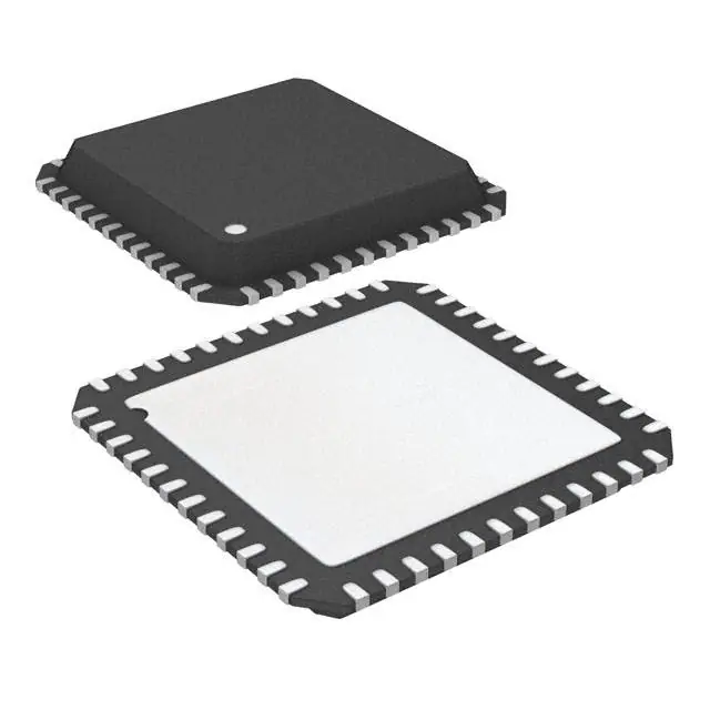
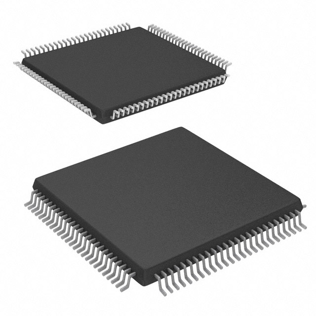
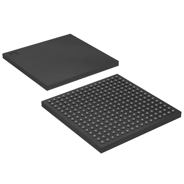
• Available in multiple package options
- 100-pin VQFP with 80 user I/O
- 144-pin TQFP with 118 user I/O
- 132-ball CP (0.5mm) BGA with 106 user I/O
- 208-pin PQFP with 173 user I/O
- 256-ball FT (1.0mm) BGA with 184 user I/O
- Pb-free available for all packages