· Standard Voltage: Vop and Vopo =1.5V±0.075V Low Voltage(L): Vop and Vopo=1.35V+0.1V,-0.067V
· High speed data transfer rates with system frequency up to 933 MHz
· 8 internal banks for concurrent operation
· 8n-Bit pre-fetch architecture
· Programmable CAS Latency
· Programmable Additive Latency:0, CL-1, CL-2
· Programmable CAS WRITE latency(CWL) based on tCK
· Programmable Burst Length:4 and 8
· Programmable Burst Sequence: Sequential or Interleave
· BL switch on the fly
· Auto Self Refresh(ASR)
· Self Refresh Temperature(SRT)
· Refresh Interval:
7.8 us(8192 cycles/64ms) Tc=40℃ to 85℃
3.9 us(8192 cycles/32 ms) Tc=85℃ to 105℃
· Partial Array Self Refresh
· Asynchronous RESET pin
· TDQS(Termination Data Strobe) supported(×8 only)
· OCD(Off-Chip Driver Impedance Adjustment)
· Dynamic ODT(On-Die Termination)
· Driver strength: RZQ/7, RZQ/6(RZQ=240 Q)
· Write Leveling
· Operating temperature:
Commercial(Tc=0C to +95℃)
Industrial(Tc=-40℃ to +95℃)
Automotive,A1(Tc=-40℃ to+95℃)
Automotive,A2(Tc=-40℃ to+105℃)
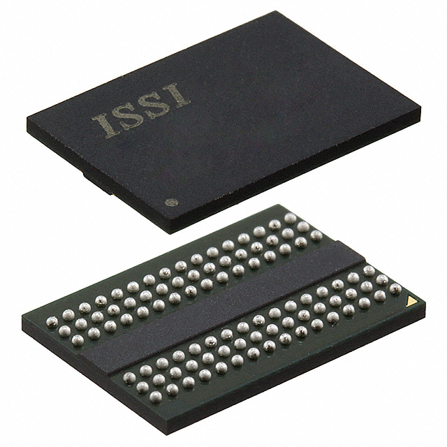
(Picture:Pinout / Diagram)