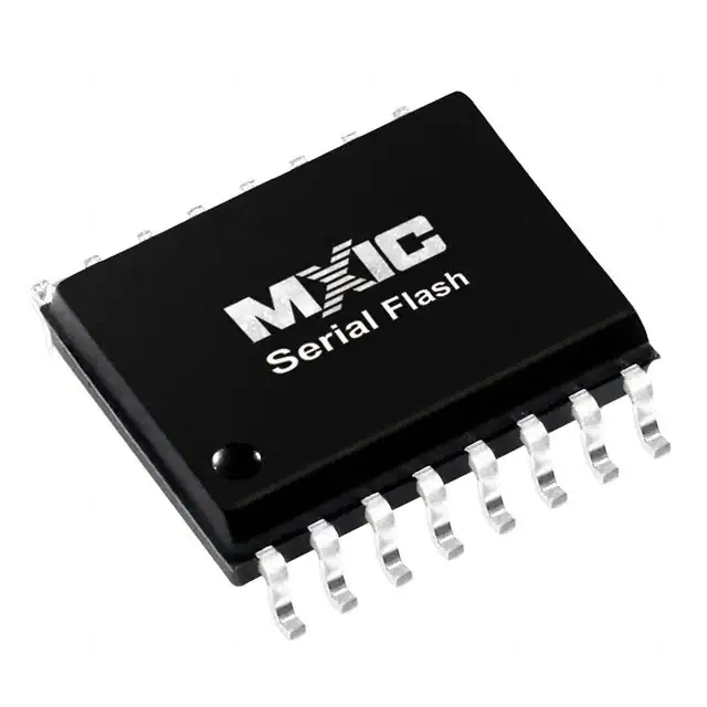
MX25V1635F is 16Mb bits Serial NOR Flash memory, which is configured as 2,097,152 x 8 internally. When it is in four I/O mode, the structure becomes 4,194,304 bits x 4 or 8,388,608 bits x 2.
MX25V1635F features a serial peripheral interface and software protocol allowing operation on a simple 3-wire bus while it is in single I/O mode. The three bus signals are a clock input (SCLK), a serial data input (SI), and a serial data output (SO). Serial access to the device is enabled by CS# input.
When it is in two I/O read mode, the SI pin and SO pin become SIO0 pin and SIO1 pin for address/dummy bits input and data output. When it is in four I/O read mode, the SI pin, SO pin, WP# pin and HOLD# pinbecome SIO0 pin, SIO1 pin, SIO2 pin and SIO3 pin for address/dummy bits input and data output.
The MX25V1635F MXSMIO® (Serial Multi I/O) provides sequential read operation on the whole chip.
After program/erase command is issued, auto program/erase algorithms which program/erase and verify the specified page or sector/block locations will be executed. Program command is executed on byte basis, or page (256 bytes) basis, or word basis. Erase command is executed on 4K-byte sector, or 32KB block (32K-byte), or 64K-byte block, or whole chip basis.
To provide user with ease of interface, a status register is included to indicate the status of the chip. The status read command can be issued to detect completion status of a program or erase operation via WIP bit.
Advanced security features enhance the protection and security functions, please see security features section for more details.
The MX25V1635F utilizes Macronix's proprietary memory cell, which reliably stores memory contents even after 100,000 program and erase cycles.
2. FEATURES
GENERAL
• Supports Serial Peripheral Interface -- Mode 0 and Mode 3
• 16,777,216 x 1 bit structure
or 8,388,608 x 2 bits (two I/O mode) structure
or 4,194,304 x 4 bits (four I/O mode) structure
• Equal Sectors with 4K byte each, Equal Blocks with 32K byte each, or Equal Blocks with 64K byte each
- Any Block can be erased individually
• Single Power Supply Operation
- Operation Voltage: 2.3V-3.6V for Read, Erase and Program Operations
• Latch-up protected to 100mA from -1V to Vcc +1V
PERFORMANCE
• High Performance
- Fast read
- 1 I/O: 80MHz with 8 dummy cycles
- 2 I/O: 80MHz with 4 dummy cycles, equivalent to 160MHz
- 4 I/O: 80MHz with 2+4 dummy cycles, equivalent to 320MHz
- Fast program and erase time
- 8/16/32/64 byte Wrap-Around Burst Read Mode
• Low Power Consumption
• Minimum 100,000 erase/program cycles
• 20 years data retention
SOFTWARE FEATURES
• Input Data Format
- 1-byte Command code
• Advanced Security Features
- Block lock protection The BP0-BP3 status bit defines the size of the area to be software protection against program and erase instructions
• Additional 8K bits secured OTP
- Features unique identifier.
- Factory locked identifiable and customer lockable
• Auto Erase and Auto Program Algorithm
- Automatically erases and verifies data at selected sector or block
- Automatically programs and verifies data at selected page by an internal algorithm that automatically times the program pulse widths (Any page to be programed should have page in the erased state first)
• Status Register Feature
• Command Reset
• Program/Erase Suspend and Program/Erase Resume
• Electronic Identification
- JEDEC 1-byte manufacturer ID and 2-byte device ID
- RES command for 1-byte Device ID
- REMS command for 1-byte manufacturer ID and 1-byte device ID
• Support Serial Flash Discoverable Parameters (SFDP) mode
• Support Unique ID (Please contact local Macronix sales for detail information)
HARDWARE FEATURES
• SCLK Input
- Serial clock input
• SI/SIO0
- Serial Data Input or Serial Data Input/Output for 2 x I/O read mode and 4 x I/O read mode
• SO/SIO1
- Serial Data Output or Serial Data Input/Output for 2 x I/O read mode and 4 x I/O read mode
• WP#/SIO2
- Hardware write protection or serial data Input/Output for 4 x I/O read mode
• HOLD#/SIO3
- HOLD feature, to pause the device without deselecting the device or Serial input & Output for 4 x I/O read mode
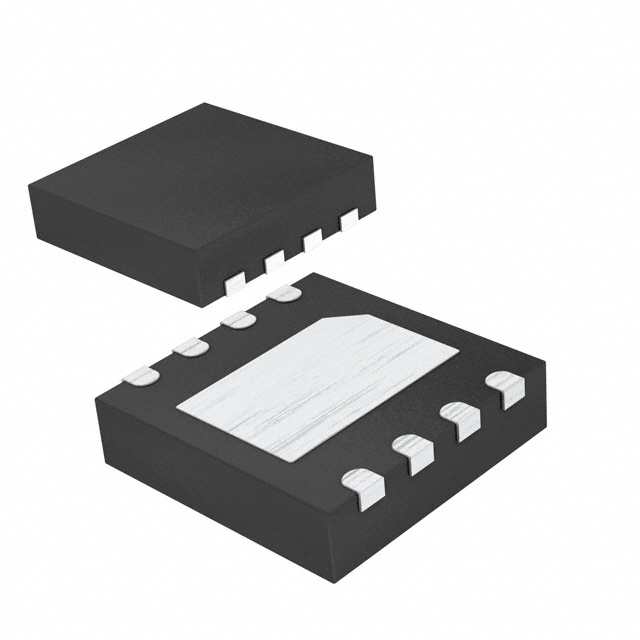
• PACKAGE
- 8-pin SOP (150mil/200mil)
- 8-land WSON (6x5mm)
- 8-land USON (4x3mm)
- 8-land USON (2x3mm)
- 24 ball TFBGA (6x8mm)
- All devices are RoHS Compliant and Halogenfree
(Picture:Pinout / Diagram)