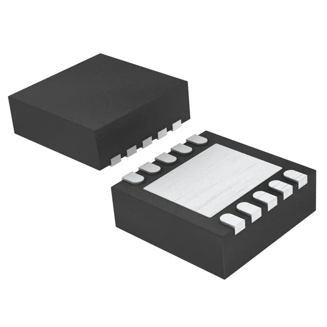
The TPS61093DSKR is a highly integrated boost regulator for up to 17-V output. In addition to the on-chip 1-A PWM switch and power diode, this IC also integrates an output-side isolation switch as shown in the functional block diagram.
One common issue with conventional boost regulators is the conduction path from input to output even when the PWM switch is turned off. It creates three problems, which are inrush current during start-up, output leakage current during shutdown, and excessive overload current.
In the TPS61093, the isolation switch turns off under shutdown-mode and overload conditions, thereby opening the current path. However, shorting the VO and OUT pins bypasses the isolation switch and enhances efficiency. Because the isolation switch is on the output side, the IC's VIN pin and power stage input power (up to 10 V) can be separated.
The TPS61093DSKR adopts current-mode control with constant pulse-width-modulation (PWM) frequency. The switching frequency is fixed at 1.2 MHz typical. PWM operation turns on the PWM switch at the beginning of each switching cycle. The input voltage is applied across the inductor and the inductor current ramps up. In this mode, the output capacitor is discharged by the load current. When the inductor current hits the threshold set by the error amplifier output, the PWM switch is turned off, and the power diode is forward-biased.
The inductor transfers its stored energy to replenish the output capacitor. This operation repeats in the next switching cycle.
The error amplifier compares the FB-pin voltage with an internal reference, and its output determines the duty cycle of the PWM switching. This closed-loop system requires frequency compensation for stable operation. The device has a built-in compensation circuit that can accommodate a wide range of input and output voltages.
To avoid the sub-harmonic oscillation intrinsic to current-mode control, the IC also integrates slope compensation,which adds an artificial slope to the current ramp.
TPS61093DSKR Applications
• 3.3-V to 12-V, 5-V to 12-V Boost Converters
Feature
- Input range: 1.6 V to 6 V
- Integrated power diode and isolation FET
- 20-V Internal switch FET with 1.1-A current
- Fixed 1.2-MHz switching frequency
- Efficiency at 15-V output up to 88%
- Overload and overvoltage protection
- Programmable soft start-up
- Load discharge path after IC shutdown
- 2.5 mm × 2.5 mm × 0.8 mm WSON package
- Create a custom design using the TPS61093 with theWEBENCH? Power Designer
All trademarks are the property of their respective owners.
DescriptionThe TPS61093 is a 1.2-MHz, fixed-frequency boost converter designed for high integrationand high reliability. The IC integrates a 20-V power switch, input/output isolation switch, andpower diode. When the output current exceeds the overload limit, the isolation switch of the ICopens up to disconnect the output from the input, thus protecting the IC and the input supply. Theisolation switch also disconnects the output from the input during shutdown to minimize leakagecurrent. When the IC is shut down, the output capacitor is discharged to a low voltage level byinternal diodes. Other protection features include 1.1-A peak overcurrent protection (OCP) at eachcycle, output overvoltage protection (OVP), thermal shutdown, and undervoltage lockout(UVLO).
With its 1.6-V minimum input voltage, the IC can be powered by two alkaline batteries, asingle Li-ion battery, or 3.3-V and 5-V regulated supply. The output can be boosted up to 17 V. TheTPS61093 is available in 2.5 mm × 2.5 mm VSON package with thermal pad.


