
All trademarks are the property of their respective owners.
DescriptionThe TPS65131-Q1 device is dual-outputdc-dc converter generating a positive output voltage up to 15 V and a negative output voltage downto –15 V with output currents of typically 200 mA, depending on input-voltage to output-voltageratio. With a total efficiency up to 85%, the device is ideal for portable battery-poweredequipment. The input-voltage range of 2.7 V to 5.5 V allows, for example, 3.3-V and 5-V rails topower the TPS65131-Q1 device. The TPS65131-Q1 device comes in a QFN-24 package with thermal pad.Requiring few and small external components, the overall solution size can be small.
The converter operates with a fixed-frequency PWM control topology and, with power-savemode enabled, uses a pulse-skipping mode at light load currents. In operation, the typical overalldevice quiescent current is only 500 μA. In shutdown, the device draws typically 0.2 μA.Independent enable pins allow power-up and power-down sequencing for both outputs. The device hasan internal current limit, overvoltage protection, and a thermal shutdown for highest reliabilityunder fault conditions.
The TPS65131-Q1 device is qualified for automotive applications, according to AEC-Q100temperature grade 2. The electrical characteristics are tested over –40°C to 125°C device junctiontemperature. This, combined with lowest shutdown currents, small solution size, package withthermal pad, plus good efficiency and protection features, targets automotive and industrialapplications.
Feature
- Qualified for Automotive Applications
- AEC-Q100 Test GuidanceWith the Following Results:
- Device Temperature Grade2: –40°C to 105°C Ambient Operating Temperature Range
- ElectricalCharacteristics Tested Over –40°C to 125°C Junction Temperature Range
- Device HBM ESD Classification LevelH1C
- Device CDM ESD Classification Level C4B
- Dual Adjustable Output Voltages up to15 V and down to –15 V
- 2–A Typical Switch-Current Limit for Boost and Inverter Main Switches
- High Conversion Efficiency
- Up to 91% at Positive Output Rail
- Up to 85% at Negative Output Rail
- Power-Save Mode at LowLoad
- Independent Enable Inputs for Power-Up and Power-Down Sequencing
- Control Output for External PFET to Support Complete Supply Disconnect When ShutDown
- 2.7-V to 5.5-V Input-Voltage Range
- Minimum 1.25-MHz Fixed-Frequency PWM Operation
- Thermal Shutdown
- Overvoltage Protection on Both Outputs
- 0.2-μA Typical Shutdown Current
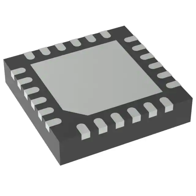
- Small 4-mm × 4-mm QFN-24 Package (RGE)
All trademarks are the property of their respective owners.
DescriptionThe TPS65131-Q1 device is dual-outputdc-dc converter generating a positive output voltage up to 15 V and a negative output voltage downto –15 V with output currents of typically 200 mA, depending on input-voltage to output-voltageratio. With a total efficiency up to 85%, the device is ideal for portable battery-poweredequipment. The input-voltage range of 2.7 V to 5.5 V allows, for example, 3.3-V and 5-V rails topower the TPS65131-Q1 device. The TPS65131-Q1 device comes in a QFN-24 package with thermal pad.Requiring few and small external components, the overall solution size can be small.
The converter operates with a fixed-frequency PWM control topology and, with power-savemode enabled, uses a pulse-skipping mode at light load currents. In operation, the typical overalldevice quiescent current is only 500 μA. In shutdown, the device draws typically 0.2 μA.Independent enable pins allow power-up and power-down sequencing for both outputs. The device hasan internal current limit, overvoltage protection, and a thermal shutdown for highest reliabilityunder fault conditions.
The TPS65131-Q1 device is qualified for automotive applications, according to AEC-Q100temperature grade 2. The electrical characteristics are tested over –40°C to 125°C device junctiontemperature. This, combined with lowest shutdown currents, small solution size, package withthermal pad, plus good efficiency and protection features, targets automotive and industrialapplications.


