
The TPS54061-Q1 device is a 60-V, 200-mA, synchronous step-down DC-DC converter with integrated high-side and low-side MOSFETs. Current-mode control provides simple external compensation and flexible component selection. The non-switching supply current is 90 μA. Using the enable pin reduces the shutdown supply current to 1.4 μA.
To increase light-load efficiency, the low-side MOSFET emulates a diode when the inductor current reaches zero.
The internal undervoltage lockout setting is 4.5 V, but using two resistors on the enable pin can increase the setting. The internal slow-start time controls the output-voltage start-up ramp.
The adjustable switching-frequency range allows optimization of efficiency and external component size. Frequency foldback and thermal shutdown protect the part during an overload condition.
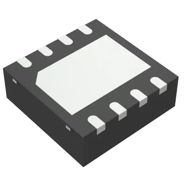
The TPS54061-Q1 enables small designs by integrating the MOSFETs and boot recharge diode, and by minimizing the IC footprint with a small 3-mm × 3-mm thermally-enhanced SON package.
The TPS54061-Q1 is supported in the WEBENCH? Designer at www.ti.com.
Feature
- Qualified for Automotive Applications
- AEC-Q100 Qualified With the Following Results:
- Device Temperature Grade 1: –40°C to 125°C Ambient Operating Temperature Range
- Device HBM ESD Classification Level H2
- Device CDM ESD Classification Level C3B
- Integrated High-Side and Low-Side MOSFETs
- Diode Emulation for Light-Load Efficiency
- Peak-Current Mode Control
- 90-μA Operating Quiescent Current
- 1.4-μA Shutdown Supply Current
- 50-kHz to 1.1-MHz Adjustable Switching Frequency
- Synchronizes to External Clock
- 0.8 V ±1% Voltage Reference
- Stable With Ceramic Output Capacitors or Low- Cost Aluminum Electrolytic
- Cycle-by-Cycle Current Limit, Thermal, OVP, and Frequency Foldback Protection
- 3-mm × 3-mm, 8-Pin SON Package With Thermal Pad
- –40°C to 150°C Operating Junction Temperature
The TPS54061-Q1 device is a 60-V, 200-mA, synchronous step-down DC-DC converter with integrated high-side and low-side MOSFETs. Current-mode control provides simple external compensation and flexible component selection. The non-switching supply current is 90 μA. Using the enable pin reduces the shutdown supply current to 1.4 μA.
To increase light-load efficiency, the low-side MOSFET emulates a diode when the inductor current reaches zero.
The internal undervoltage lockout setting is 4.5 V, but using two resistors on the enable pin can increase the setting. The internal slow-start time controls the output-voltage start-up ramp.
The adjustable switching-frequency range allows optimization of efficiency and external component size. Frequency foldback and thermal shutdown protect the part during an overload condition.
The TPS54061-Q1 enables small designs by integrating the MOSFETs and boot recharge diode, and by minimizing the IC footprint with a small 3-mm × 3-mm thermally-enhanced SON package.
The TPS54061-Q1 is supported in the WEBENCH? Designer at www.ti.com.


