
All trademarks are the property of their respective owners.
DescriptionTheTPS62748YFPT is a high efficiency stepdown converter with ultra low quiescent current of typical 360 nA. The device is optimized tooperate with a 2.2-μH inductor and 10μF output capacitor. The device uses DCS-Control? and operateswith a typical switching frequency of 1.2 MHz. In Power Save Mode the device extends the light loadefficiency down to a load current range of 10-μA and below. TPS62748YFPT provides an output currentof 300 mA. Oncestarted the device operates down to an input voltage range of 2.0 V. This allows to operate thedevice directly from a single Li-MnO2 coin cell.
The TPS62748YFPT provides two programmableoutput voltages of 1.2V and 1.8V selectable by one voltage select pin. The TPS62748YFPT is optimized to provide alow output voltage ripple and low noise using a small output capacitor. Once the input voltagecomes close to the output voltage the device enters the No Ripple 100% mode to prevent an increaseof output ripple voltage. In this operation mode the device stops switching and turns the high sideMOSFET switch on.
The TPS62748YFPT has a 100 mA load switch between pins VOS and LOAD with atypical ON-resistance of 0.6 Ohm. The load switch is typically used to distribute the buckconverter output voltage to the sub-system.
Feature
- Input Voltage RangeVIN from 2.15 V to 5.5 V
- Input Voltage Range Down to 2.0V Once Started
- 300 mA Output Current
- 360 nA Operational QuiescentCurrent
- Up to 90% Efficiency at 10-μA OutputCurrent
- Power Save Mode Operation
- Selectable OutputVoltages
- 1.2 V and 1.8 V
- Output Voltage Discharge
- 100 mA/2.2 Ω Integrated Load Switch
- Low Output VoltageRipple
- Automatic Transition to No Ripple 100% Mode
- RFFriendly DCS-Control?
- Total Solution Size<10mm2
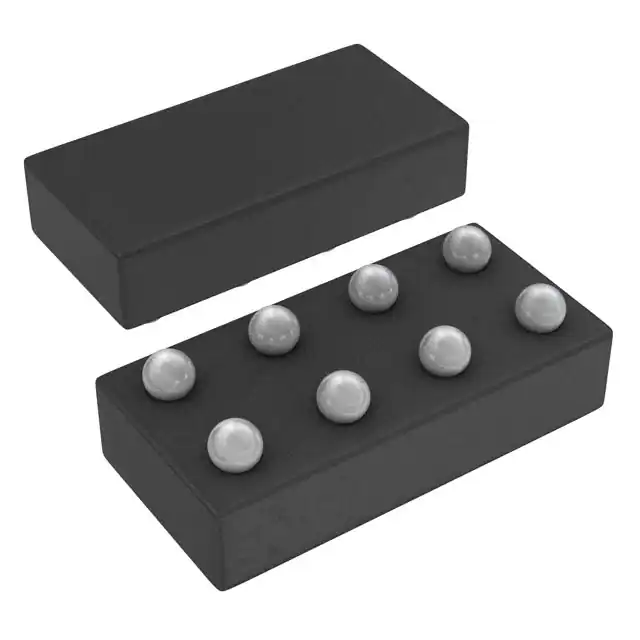
- Small 1.6 mm × 0.9 mm, 8 Ball WCSP Package
All trademarks are the property of their respective owners.
DescriptionTheTPS62748 is a high efficiency stepdown converter with ultra low quiescent current of typical 360 nA. The device is optimized tooperate with a 2.2-μH inductor and 10μF output capacitor. The device uses DCS-Control? and operateswith a typical switching frequency of 1.2 MHz. In Power Save Mode the device extends the light loadefficiency down to a load current range of 10-μA and below. TPS62748 provides an output currentof 300 mA. Oncestarted the device operates down to an input voltage range of 2.0 V. This allows to operate thedevice directly from a single Li-MnO2 coin cell.
The TPS62748 provides two programmableoutput voltages of 1.2V and 1.8V selectable by one voltage select pin. The TPS62748 is optimized to provide alow output voltage ripple and low noise using a small output capacitor. Once the input voltagecomes close to the output voltage the device enters the No Ripple 100% mode to prevent an increaseof output ripple voltage. In this operation mode the device stops switching and turns the high sideMOSFET switch on.
The TPS62748 has a 100 mA load switch between pins VOS and LOAD with atypical ON-resistance of 0.6 Ohm. The load switch is typically used to distribute the buckconverter output voltage to the sub-system.


