
All trademarks are the property of their respective owners.
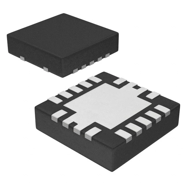
DescriptionThe TPS54620RHLT in thermally enhanced 3.50 mm × 3.50 mm QFN package is a full featured 17-V,6-A, synchronous, step-down converter which is optimized for small designs through high efficiencyand integrating the high-side and low-side MOSFETs. Further space savings are achieved throughcurrent mode control, which reduces component count, and by selecting a high switching frequency,reducing the footprint of the inductor.
The output voltage start-up ramp is controlled by the SS/TR pin which allows operation aseither a stand-alone power supply or in tracking situations. Power sequencing is also possible bycorrectly configuring the enable and the open-drain power good pins.
Cycle-by-cycle current limiting on the high-side FET protects the device in overloadsituations and is enhanced by a low-side sourcing current limit which prevents current runaway.There is also a low-side sinking current limit that turns off the low-side MOSFET to preventexcessive reverse current. Thermal shutdown disables the part when die temperature exceeds thermalshutdown temperature.
Feature
- Integrated 26 m? and 19 m? MOSFETs
- Split Power Rail: 1.6 V to 17 V on PVIN
- 200-kHz to 1.6-MHz Switching Frequency
- Synchronizes to External Clock
- 0.8 V ±1% Voltage Reference Overtemperature
- Low 2-μA Shutdown Quiescent Current
- Monotonic Start-Up into Prebiased Outputs
- –40°C to 150°C Operating Junction Temperature Range
- Adjustable Slow Start and Power Sequencing
- Power Good Output Monitor for Undervoltage and Overvoltage
- Adjustable Input Undervoltage Lockout
- For SWIFT? Documentation, Visit http://www.ti.com/swift
- Create a Custom Design Using the TPS54620 With theWEBENCHPower Designer
All trademarks are the property of their respective owners.
DescriptionThe TPS54620 in thermally enhanced 3.50 mm × 3.50 mm QFN package is a full featured 17-V,6-A, synchronous, step-down converter which is optimized for small designs through high efficiencyand integrating the high-side and low-side MOSFETs. Further space savings are achieved throughcurrent mode control, which reduces component count, and by selecting a high switching frequency,reducing the footprint of the inductor.
The output voltage start-up ramp is controlled by the SS/TR pin which allows operation aseither a stand-alone power supply or in tracking situations. Power sequencing is also possible bycorrectly configuring the enable and the open-drain power good pins.
Cycle-by-cycle current limiting on the high-side FET protects the device in overloadsituations and is enhanced by a low-side sourcing current limit which prevents current runaway.There is also a low-side sinking current limit that turns off the low-side MOSFET to preventexcessive reverse current. Thermal shutdown disables the part when die temperature exceeds thermalshutdown temperature.


