
All trademarks are the property of their respective owners.
DescriptionThis single 2-input positive-AND gate is designed for 1.65-V to 5.5-VVCC operation.
The SN74LVC1G08-Q1 device performs the Boolean function orin positive logic.
This device is fully specified for partial-power-down applications using I off. The I offcircuitry disables the outputs, preventing damaging current backflow through the device when it ispowered down.
The CMOS device has high output drive while maintaining low static power dissipation overa broad VCC operating range.
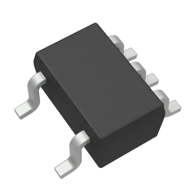
The SN74LVC1G08QDCKRQ1 is available in a variety of packages, including the small DRY packagewith a body size of 1.45 mm × 1.00 mm.
Feature
- AEC-Q100 Qualified for Automotive Applications:
- Device Temperature Grade 1: –40°C to +125°C, TA
- Supports 5-V VCC Operation
- Over-voltage Tolerant Inputs Accept Voltages to 5.5 V
- Provides Down Translation to VCC
- Low Power Consumption, 10-μA Max ICC
- ±24-mA Output Drive at 3.3 V
- Ioff Supports Live Insertion, Partial-Power-Down Mode, andBack Drive Protection
- Latch-Up Performance Exceeds 100 mA Per JESD 78, Class II
- ESD Protection Exceeds JESD 22
- 2000-V Human-Body Model (A114-A)
- 200-V Machine Model (A115-A)
- 1000-V Charged-Device Model (C101)
All trademarks are the property of their respective owners.
DescriptionThis single 2-input positive-AND gate is designed for 1.65-V to 5.5-VVCC operation.
The SN74LVC1G08-Q1 device performs the Boolean function orin positive logic.
This device is fully specified for partial-power-down applications using I off. The I offcircuitry disables the outputs, preventing damaging current backflow through the device when it ispowered down.
The CMOS device has high output drive while maintaining low static power dissipation overa broad VCC operating range.
The SN74LVC1G08 is available in a variety of packages, including the small DRY packagewith a body size of 1.45 mm × 1.00 mm.


