
All trademarks are the property of their respective owners.
DescriptionThis single 2-input positive-OR gate is designed for 1.65-V to5.5-V VCC operation.
The SN74LVC1G32-Q1 device performs the Boolean functionin positive logic.
The CMOS device has high output drive while maintaining low static power dissipation overa broad VCC operating range.
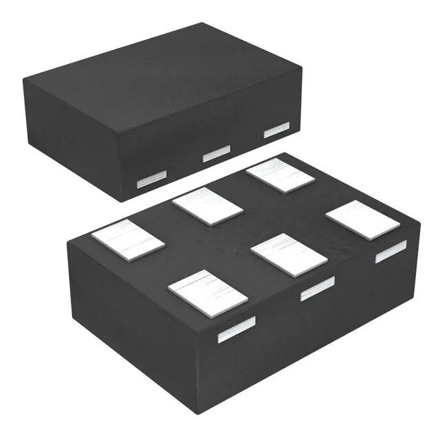
The SN74LVC1G32-Q1 device is available in a variety of packages, including the small DRYpackage with a body size of 1.45 × 1.00 mm.
Feature
- Available in the small 1.45 mm2 Package (DRY) with 0.5-mm Pitch
- Supports 5-V VCC Operation
- Inputs Accept Voltages to 5.5-V
- Supports Down Translation to VCC
- Maxtpd of 3.6 ns at 3.3-V
- Low Power Consumption, 10-μA Max ICC
- ±24-mA Output Drive at 3.3-V
- Ioff Supports Live Insertion, Partial-Power-Down Mode, andBack-Drive Protection
- Latch-Up Performance Exceeds 100 mA Per JESD 78, Class II
- ESD Protection Exceeds JESD 22
- 2000-V Human-Body Model (A114-A)
- 200-V Machine Model (A115-A)
- 1000-V Charged-Device Model (C101)
All trademarks are the property of their respective owners.
DescriptionThis single 2-input positive-OR gate is designed for 1.65-V to5.5-V VCC operation.
The SN74LVC1G32-Q1 device performs the Boolean functionin positive logic.
The CMOS device has high output drive while maintaining low static power dissipation overa broad VCC operating range.
The SN74LVC1G32-Q1 device is available in a variety of packages, including the small DRYpackage with a body size of 1.45 × 1.00 mm.


