
* FAST is a Registered Trademark of Fairchild Semiconductor Corp.
DescriptionThe RCA CD54/74AC651 and CD54/74AC652 and the CD54/74ACT651 and CD54/74ACT652 3-state, octal-bus transceiver/registers use the RCA ADVANCED CMOS technology. The CD54/74AC651 and CD54/74ACT651 have inverting outputs. The CD54/74AC562 and CD54/74ACT652 have non-inverting outputs. These devices consist of bus tranceiver circuits, D-type flip-flops, and control circuitry arranged for multiplexed transmission of data directly from the data bus or from the internal storage registers. Output Enables OEAB and OE\BA are provided to control the transceiver functions. SAB and SBA control pins are provided to select whether real-time or stored data is transferred. The circuitry used for select control will eliminate the typical decoding glitch that occurs in a multiplexer during the transition between stored and real-time data. A LOW input level selects real-time data, and a HIGH selects stored data. The following examples demonstrate the four fundamental bus-management functions that can be performed with the octal-bus transceivers and registers.
Data on the A or B data bus, or both, can be stored in the internal D flip-flops by low-to-high transitions at the appropriate clock pins (CAB or CBA) regardless of the select or enable control pins. When SAB and SBA are in the real-time transfer mode, it is also possible to store data without using the internal D-type flip-flops by simultaneously enabling OEAB and OE\BA. In this configuration, each output reinforces its input. Thus, when all other data sources to the two sets of bus lines are a high impedance, each set of bus lines will remain at its last state.
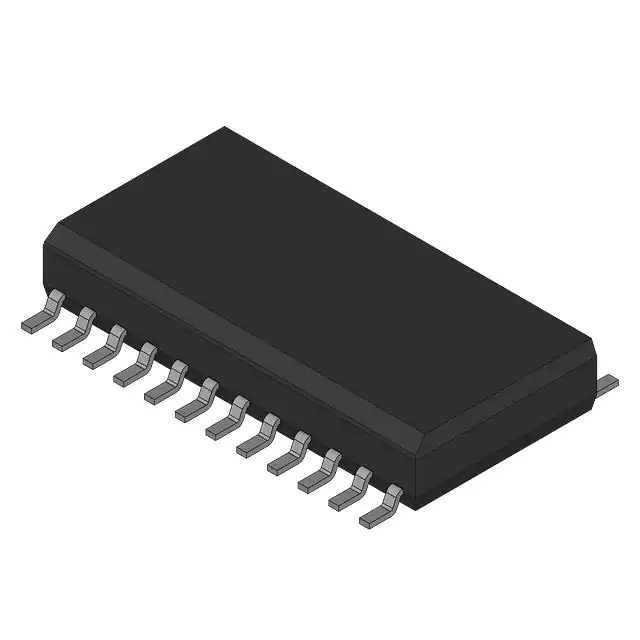
The CD74AC/ACT651 and CD74AC/ACT652 are supplied in 24-lead dual-in-line narrow-body plastic packages (EN suffix) and in 24-lead dual-in-line small-outline plastic packages (M suffix). Both package ty0es are operable over the following temperature ranges. Commerical (0 to 70°C); industrial (-40 to +85°C); and Extended Industrial/Military (-55 to +125°C).
The CD54AC/ACT651 and CD54AC/ACT652, available in chip form (H suffix), are operable over the -55 to +125°C temperature range.
Feature
- Buffered inputs
- Typical propagation delay:
- 5.3 ns @ VCC = 5 V, TA = 25°C, CL = 50 pF
- Exceeds 2-kV ESD Protection - MIL-STD-883, Method 3015
- SCR-Latchup-resistant CMOS process and circuit design
- Speed of bipolar FAST*/AS/S with significantly reduced power consumption
- Balanced propagation delays
- AC types feature 1.5-V to 5.5-V operation and balanced noise immunity at 30% of the supply
- ± 24-mA output drive current
- Fanout of 15 FAST* ICs
- Drives 50-ohm transmission lines
- Characterized for operation from –40° to 85°C
* FAST is a Registered Trademark of Fairchild Semiconductor Corp.
DescriptionThe RCA CD54/74AC651 and CD54/74AC652 and the CD54/74ACT651 and CD54/74ACT652 3-state, octal-bus transceiver/registers use the RCA ADVANCED CMOS technology. The CD54/74AC651 and CD54/74ACT651 have inverting outputs. The CD54/74AC562 and CD54/74ACT652 have non-inverting outputs. These devices consist of bus tranceiver circuits, D-type flip-flops, and control circuitry arranged for multiplexed transmission of data directly from the data bus or from the internal storage registers. Output Enables OEAB and OE\BA are provided to control the transceiver functions. SAB and SBA control pins are provided to select whether real-time or stored data is transferred. The circuitry used for select control will eliminate the typical decoding glitch that occurs in a multiplexer during the transition between stored and real-time data. A LOW input level selects real-time data, and a HIGH selects stored data. The following examples demonstrate the four fundamental bus-management functions that can be performed with the octal-bus transceivers and registers.
Data on the A or B data bus, or both, can be stored in the internal D flip-flops by low-to-high transitions at the appropriate clock pins (CAB or CBA) regardless of the select or enable control pins. When SAB and SBA are in the real-time transfer mode, it is also possible to store data without using the internal D-type flip-flops by simultaneously enabling OEAB and OE\BA. In this configuration, each output reinforces its input. Thus, when all other data sources to the two sets of bus lines are a high impedance, each set of bus lines will remain at its last state.
The CD74AC/ACT651 and CD74AC/ACT652 are supplied in 24-lead dual-in-line narrow-body plastic packages (EN suffix) and in 24-lead dual-in-line small-outline plastic packages (M suffix). Both package ty0es are operable over the following temperature ranges. Commerical (0 to 70°C); industrial (-40 to +85°C); and Extended Industrial/Military (-55 to +125°C).
The CD54AC/ACT651 and CD54AC/ACT652, available in chip form (H suffix), are operable over the -55 to +125°C temperature range.


