
The TMS320C6203BGNZ173 device is part of the TMS320C62x fixed-point DSP generation in the TMS320C6000 DSP platform. The C62x DSP devices are based on the high-performance, advanced VelociTI very-long-instruction-word (VLIW) architecture developed by Texas Instruments (TI), making these DSPs an excellent choice for multichannel and multifunction applications.
The TMS320C62x DSP offers cost-effective solutions to high-performance DSP-programming challenges. The TMS320C6203BGNZ173 has a performance capability of up to 2400 MIPS at a clock rate of 300 MHz. The C6203B DSP possesses the operational flexibility of high-speed controllers and the numerical capability of array processors. This processor has 32 general-purpose registers of 32-bit word length and eight highly independent functional units. The eight functional units provide six arithmetic logic units (ALUs) for a high degree of parallelism and two 16-bit multipliers for a 32-bit result. The C6203B can produce two multiply-accumulates (MACs) per cycle for a total of 600 million MACs per second (MMACS). The C6203B DSP also has application-specific hardware logic, on-chip memory, and additional on-chip peripherals.
The C6203B device program memory consists of two blocks, with a 256K-byte block configured as memory-mapped program space, and the other 128K-byte block user-configurable as cache or memory-mapped program space. Data memory for the C6203B consists of two 256K-byte blocks of RAM.
The C6203B device has a powerful and diverse set of peripherals. The peripheral set includes three multichannel buffered serial ports (McBSPs), two general-purpose timers, a 32-bit expansion bus (XBus) that offers ease of interface to synchronous or asynchronous industry-standard host bus protocols, and a glueless 32-bit external memory interface (EMIF) capable of interfacing to SDRAM or SBSRAM and asynchronous peripherals.
The C62x devices have a complete set of development tools which includes: a new C compiler, an assembly optimizer to simplify programming and scheduling, and a Windows debugger interface for visibility into source code execution.
Feature
- High-Performance Fixed-Point Digital Signal Processor (DSP) - TMS320C62x
- 4-, 3.33-ns Instruction Cycle Time
- 250-, 300-MHz Clock Rate
- Eight 32-Bit Instructions/Cycle
- 2000, 2400 MIPS
- C6203B and C6202 GLS Ball Grid Array (BGA) Packages are Pin-Compatible With the C6204 GLW BGA Package
- C6203B and C6202B GNZ, GNY and ZNY Packages are Pin-Compatible
- VelociTI Advanced Very-Long-Instruction-Word (VLIW) C62x DSP Core
- Eight Highly Independent Functional Units:
- Six ALUs (32-/40-Bit)
- Two 16-Bit Multipliers (32-Bit Result)
- Load-Store Architecture With 32 32-Bit General-Purpose Registers
- Instruction Packing Reduces Code Size
- All Instructions Conditional
- Eight Highly Independent Functional Units:
- Instruction Set Features
- Byte-Addressable (8-, 16-, 32-Bit Data)
- 8-Bit Overflow Protection
- Saturation
- Bit-Field Extract, Set, Clear
- Bit-Counting
- Normalization
- 7M-Bit On-Chip SRAM
- 3M-Bit Internal Program/Cache (96K 32-Bit Instructions)
- 4M-Bit Dual-Access Internal Data (512K Bytes)
- Organized as Two 256K-Byte Blocks for Improved Concurrency
- 32-Bit External Memory Interface (EMIF)
- Glueless Interface to Synchronous Memories: SDRAM or SBSRAM
- Glueless Interface to Asynchronous Memories: SRAM and EPROM
- 52M-Byte Addressable External Memory Space
- Four-Channel Bootloading Direct-Memory-Access (DMA) Controller With an Auxiliary Channel
- Flexible Phase-Locked-Loop (PLL) Clock Generator
- 32-Bit Expansion Bus (XBus)
- Glueless/Low-Glue Interface to Popular PCI Bridge Chips
- Glueless/Low-Glue Interface to Popular Synchronous or Asynchronous Microprocessor Buses
- Master/Slave Functionality
- Glueless Interface to Synchronous FIFOs and Asynchronous Peripherals
- Three Multichannel Buffered Serial Ports (McBSPs)
- Direct Interface to T1/E1, MVIP, SCSA Framers
- ST-Bus-Switching Compatible
- Up to 256 Channels Each
- AC97-Compatible
- Serial-Peripheral Interface (SPI) Compatible (Motorola)
- Two 32-Bit General-Purpose Timers
- IEEE-1149.1 (JTAG) Boundary-Scan-Compatible
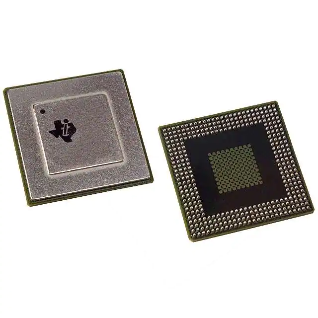
- 352-Pin BGA Package (GNZ)
- 384-Pin BGA Package (GLS)
- 384-Pin BGA Package (GNY and ZNY)
- 0.15-μm/5-Level Metal Process
- CMOS Technology
- 3.3-V I/Os, 1.5-V Internal


