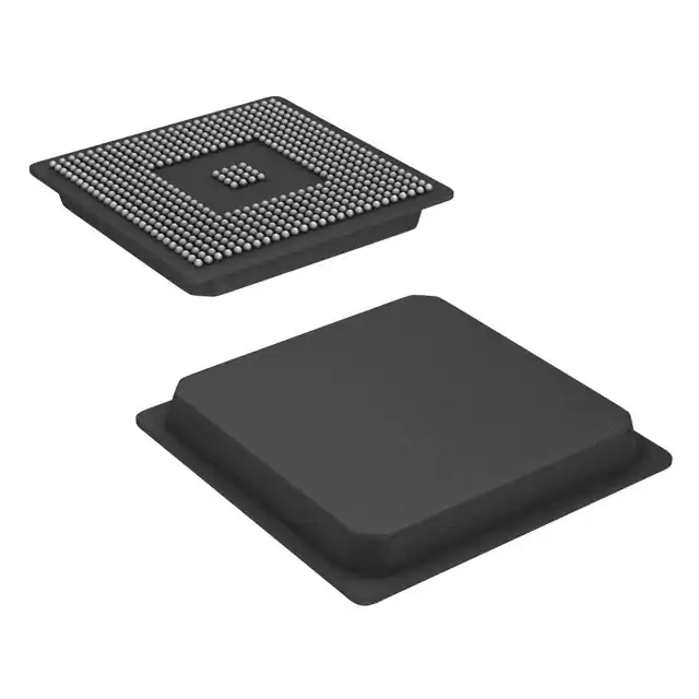
The TMS320C64xDSPs (including the TMS320C6412AZNZ6 device) are thehighest-performance fixed-point DSP generation in the TMS320C6000 DSP platform.The TMS320C6412AZNZ6 (C6412) device is based on the second-generationhigh-performance, advanced VelociTI very-long-instruction-word (VLIW)architecture (VelociTI.2) developed by Texas Instruments (TI), making theseDSPs an excellent choice for digital media applications. The C64x is acode-compatible member of the C6000 DSP platform.
With performance of up to 5760 million instructions per second (MIPS) at aclock rate of 720 MHz, the C6412 device offers cost-effective solutions tohigh-performance DSP programming challenges. The C6412 DSP possesses theoperational flexibility of high-speed controllers and the numerical capabilityof array processors. The C64x DSP core processor has 64 general-purposeregisters of 32-bit word length and eight highly independent functionalunits-two multipliers for a 32-bit result and six arithmetic logic units(ALUs)-with VelociTI.2 extensions. The VelociTI.2 extensions in the eightfunctional units include new instructions to accelerate the performance inapplications and extend the parallelism of the VelociTI architecture. The C6412can produce four 16-bit multiply-accumulates (MACs) per cycle for a total of2400 million MACs per second (MMACS), or eight 8-bit MACs per cycle for a totalof 4800 MMACS. The C6412 DSP also has application-specific hardware logic,on-chip memory, and additional on-chip peripherals similar to the other C6000DSP platform devices.
The C6412 uses a two-level cache-based architecture and has a powerful anddiverse set of peripherals. The Level 1 program cache (L1P) is a 128-Kbit directmapped cache and the Level 1 data cache (L1D) is a- 128-Kbit 2-wayset-associative cache. The Level 2 memory/cache (L2) consists of an 2-Mbitmemory space that is shared between program and data space. L2 memory can beconfigured as mapped memory, cache, or combinations of the two. The peripheralset includes: a 10/100 Mb/s Ethernet MAC (EMAC); a management data input/output(MDIO) module; an inter-integrated circuit (I2C) Bus module; two multichannelbuffered serial ports (McBSPs); three 32-bit general-purpose timers; auser-configurable 16-bit or 32-bit host-port interface (HPI16/HPI32); aperipheral component interconnect (PCI); a 16-pin general-purpose input/outputport (GP0) with programmable interrupt/event generation modes; and a 64-bitglueless external memory interface (EMIFA), which is capable of interfacing tosynchronous and asynchronous memories and peripherals.
The ethernet media access controller (EMAC) provides an efficient interfacebetween the C6412 DSP core processor and the network. The C6412 EMAC supportboth 10Base-T and 100Base-TX, or 10 Mbits/second (Mbps) and 100 Mbps in eitherhalf- or full-duplex, with hardware flow control and quality of service (QOS)support. The C6412 EMAC makes use of a custom interface to the DSP core thatallows efficient data transmission and reception. For more details on the EMAC,see the TMS320C6000 DSP Ethernet Media Access Controller (EMAC) / ManagementData Input/Output (MDIO) Module Reference Guide (literature numberSPRU628).
The management data input/output (MDIO) module continuously polls all 32 MDIOaddresses in order to enumerate all PHY devices in the system. Once a PHYcandidate has been selected by the DSP, the MDIO module transparently monitorsits link state by reading the PHY status register. Link change events are storedin the MDIO module and can optionally interrupt the DSP, allowing the DSP topoll the link status of the device without continuously performing costly MDIOaccesses. For more details on the MDIO port, see the TMS320C6000 DSPEthernet Media Access Controller (EMAC) / Management Data Input/Output (MDIO)Module Reference Guide (literature number SPRU628).
The I2C0 port on the TMS320C6412AZNZ6 allows the DSP to easily control peripheraldevices and communicate with a host processor. In addition, the standardmultichannel buffered serial port (McBSP) may be used to communicate with serialperipheral interface (SPI) mode peripheral devices.
The C6412 has a complete set of development tools which includes: a new Ccompiler, an assembly optimizer to simplify programming and scheduling, and aWindows debugger interface for visibility into source code
Feature
- High-Performance Digital Media Processor (TMS320C6412)
- 2-, 1.67-, 1.39-ns Instruction Cycle Time
- 500-, 600-, 720-MHz Clock Rate
- Eight 32-Bit Instructions/Cycle
- 4000, 4800, 5760 MIPS
- Fully Software-Compatible With C64x
- VelociTI.2 Extensions to VelociTI Advanced Very-Long-Instruction-Word (VLIW) TMS320C64x DSP Core
- Eight Highly Independent Functional Units With VelociTI.2 Extensions:
- Six ALUs (32-/40-Bit), Each Supports Single 32-Bit, Dual 16-Bit, or Quad 8-Bit Arithmetic per Clock Cycle
- Two Multipliers Support Four 16 x 16-Bit Multiplies (32-Bit Results) per Clock Cycle or Eight 8 x 8-Bit Multiplies (16-Bit Results) per Clock Cycle
- Load-Store Architecture With Non-Aligned Support
- 64 32-Bit General-Purpose Registers
- Instruction Packing Reduces Code Size
- All Instructions Conditional
- Eight Highly Independent Functional Units With VelociTI.2 Extensions:
- Instruction Set Features
- Byte-Addressable (8-/16-/32-/64-Bit Data)
- 8-Bit Overflow Protection
- Bit-Field Extract, Set, Clear
- Normalization, Saturation, Bit-Counting
- VelociTI.2 Increased Orthogonality
- L1/L2 Memory Architecture
- 128K-Bit (16K-Byte) L1P Program Cache (Direct Mapped)
- 128K-Bit (16K-Byte) L1D Data Cache (2-Way Set-Associative)
- 2M-Bit (256K-Byte) L2 Unified Mapped RAM/Cache (Flexible RAM/Cache Allocation)
- Endianess: Little Endian, Big Endian
- 64-Bit External Memory Interface (EMIF)
- Glueless Interface to Asynchronous Memories (SRAM and EPROM) and Synchronous Memories (SDRAM, SBSRAM, ZBT SRAM, and FIFO)
- 1024M-Byte Total Addressable External Memory Space
- Enhanced Direct-Memory-Access (EDMA) Controller (64 Independent Channels)
- 10/100 Mb/s Ethernet MAC (EMAC)
- IEEE 802.3 Compliant
- Media Independent Interface (MII)
- 8 Independent Transmit (TX) and 1 Receive (RX) Channel
- Management Data Input/Output (MDIO)
- Host-Port Interface (HPI) [32-/16-Bit]
- 32-Bit/66-MHz, 3.3-V Peripheral Component Interconnect (PCI) Master/Slave Interface Conforms to PCI Specification 2.2
- Inter-Integrated Circuit (I2C) Bus
- Two Multichannel Buffered Serial Ports
- Three 32-Bit General-Purpose Timers
- Sixteen General-Purpose I/O (GPIO) Pins
- Flexible PLL Clock Generator
- IEEE-1149.1 (JTAG) Boundary-Scan-Compatible
- 548-Pin Ball Grid Array (BGA) Package (GDK and ZDK Suffixes), 0.8-mm Ball Pitch
- 548-Pin Ball Grid Array (BGA) Package (GNZ and ZNZ Suffixes), 1.0-mm Ball Pitch
- 0.13-μm/6-Level Cu Metal Process (CMOS)
- 3.3-V I/Os, 1.2-V Internal (-500)
- 3.3-V I/Os, 1.4-V Internal (A-500, -600, -720)


