
All trademarks are the property of their respective owners.
DescriptionThe TLV62065-Q1 device is a highly-efficient synchronous step-down DC-DC converter with adjustable output voltage. The device operates at a switching frequency of 3 MHz andprovides up to 2 A of output current.
With an input voltage range of 2.9 to 5.5 V, the device is a perfect fit for power conversion from a 5-V or 3.3-V system supply rail. The TLV62065-Q1 device enters power-save mode operation at light-load currents to maintain high efficiency over the entire load current range. For low-noise applications, the TLV62065-Q1 device can be forced into fixed-frequency PWM mode by pulling the MODE pin high.
In the shutdown mode, the current consumption is reduced to less than 1 μA and an internal circuit discharges the output capacitor.
The TLV62065-Q1 device operates with a 1-μH inductor and 10-μF output capacitor.
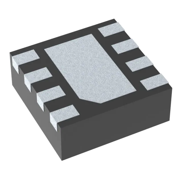
The TLV62065-Q1 device is available in a small 2-mm × 2-mm × 0.75-mm 8-pin WSON package.
For all available packages, see the orderable addendum at the end of the datasheet.
Feature
- Qualified for Automotive Applications
- AEC-Q100 Test Guidance With the Following Results:
- Device Temperature Grade 2: –40°C to +105°C Ambient Operating Temperature Range
- Device HBM ESD Classification Level 2
- Device CDM ESD Classification Level C4B
- VIN Range from 2.9 to 5.5 V
- Up to 97% Efficiency
- Power-Save Mode or Fixed Frequency PWM Mode
- Output Voltage Accuracy in PWM Mode ±2%
- Output Capacitor Discharge Function
- Typical 18-μA Quiescent Current
- 100% Duty Cycle for Lowest Dropout
- Clock Dithering
- Available in a 2-mm × 2-mm × 0.75-mm WSON
All trademarks are the property of their respective owners.
DescriptionThe TLV62065-Q1 device is a highly-efficient synchronous step-down DC-DC converter with adjustable output voltage. The device operates at a switching frequency of 3 MHz andprovides up to 2 A of output current.
With an input voltage range of 2.9 to 5.5 V, the device is a perfect fit for power conversion from a 5-V or 3.3-V system supply rail. The TLV62065-Q1 device enters power-save mode operation at light-load currents to maintain high efficiency over the entire load current range. For low-noise applications, the TLV62065-Q1 device can be forced into fixed-frequency PWM mode by pulling the MODE pin high.
In the shutdown mode, the current consumption is reduced to less than 1 μA and an internal circuit discharges the output capacitor.
The TLV62065-Q1 device operates with a 1-μH inductor and 10-μF output capacitor.
The TLV62065-Q1 device is available in a small 2-mm × 2-mm × 0.75-mm 8-pin WSON package.
For all available packages, see the orderable addendum at the end of the datasheet.


